At AsteelFlash, every one of our 18 facilities have identical equipment and processes globally allowing industrialization but also smooth transition to another facility. AsteelFlash can also adapt to special customer requests. Here are the main processes and standardized tests that are made on each PCBA before leaving our plants.
Our standard PCBA Manufacturing Process
Manufacturing of Surface Mounted Devices (SMDs) is highly automated and a production monitoring is made on each card, thanks to a manufacturing execution system (MES).
From supply to testing, here are 7 different operations realized :
 1. The screen printing : the first step of PCB manufacturing is screen printing (or stencil printing). The solder paste is put on the printed wiring board in order to establish electrical connections. The duration of this step does not depend on the size of the PCB, and the cycle time is around 30 seconds.
- 2. The solder paste inspection (SPI) : production lines are equipped with 3D optical inspection machines that scan the PCB to verify if the volume of deposited paste complies with the standards. If there is a lack of paste, the entire process is repeated to avoid any failure.
- 3. Placement of components on PCBs : components listed on the Bill of Materials (BOM) are placed on PCBs by several robot modules. Production lines can be expanded or shortened, depending on the number of components on the PCB. Machines are calibrated to fit the cycle time of the screen printing step.
- 4. Solder melting : PCBAs go through a tunnel reflow oven at 220-230 °C to melt the paste and form a solder joint. The temperature increases slowly to avoid thermal shocks that could damage components. The PCBA is then slowly cooled down and the metallic joint solidifies.
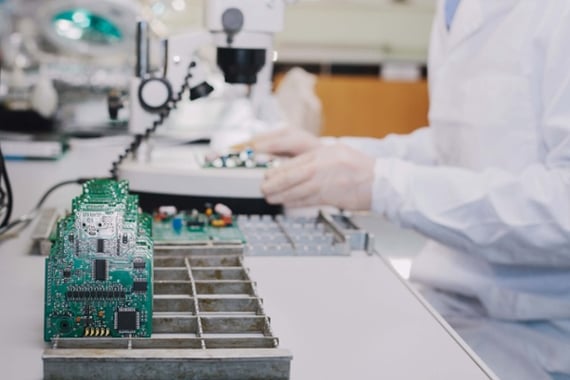
- 5. Automatic optical inspection (AOI) : another inspection step takes place to inspect the components and verify if they are still on the board. The polarity is verified as well as the size of the solder joint. Unlike SPI, AOI is fully automated.
- 6. Double-sided PCBs : for a double-sided assembly, the board is flipped and the entire process starts again. If there are heavy components on the other side, it must be bonded to prevent falling.
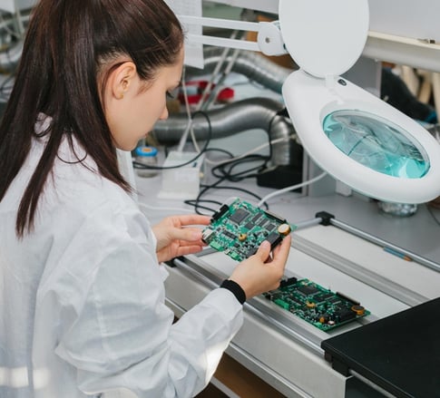
- 7. Manual operations : the PCBA manufacturing process can’t always be fully automated, especially for “high mix, low volumes”. Some components are complex to assemble requiring manual integration through a soldering iron. It’s usually the case with most of the mechanical operations like screwing or heat dissipators assembly.

Inspection tests of PCBA
Electrical tests are systematically performed before sending a product to a customer. They are of two kinds and complementary: functional and in-circuit test. The choice of tests AsteelFlash makes is set up per the customer quality requirements in the upstream design stage.
The functional test : the functionalities of the PCBA are tested. Asteelflash engineers develop test benches that reproduce the functional aspects of the product. For example, if there is a display, the testing tool verifies that the testing commands display the right information on the screen.
In-circuit test : this type of test is used to verify the components conformity on the board, as per the BOM. It can detect if a component is deficient or not.
There are two ways of making an in-circuit test :
- ICT : all the components are tested at the same time. It’s a very efficient operation that only lasts a few seconds. However, it’s expensive because it requires specific equipment only usable for one specific board. It is usually advised for larger quantities.
- Flying Probe : components are all tested one by one with a flying probe. Tests are much longer (30 minutes easily) but don’t require specific equipment. The machine is programmed depending on the board layout to test each component. It’s adapted for small runs.
Through our years of experience, Asteelflash have been continuously working on the quality of their services to offer the best experience possible.
Special processes
In addition to the standard operations, AsteelFlash can provide special processes if the customer requires them.
This include :
- Soldering push-through components
In most cases, PCBA are surface-mount devices (SMD), but in the case of push-through components, wave soldering can be used. In this process, an alloy bath licks the underside of the PCBA instead of using a solder paste.
Another process, called selective soldering can also be used. It’s the evolution of wave soldering. The alloy is brought by a nozzle mounted on a robot that moves between the melting points allowing specific points only to be soldered.
- Finishing Processes
After inspection tests, cards can undergo special treatments such as conformal coating. This treatment is used to protect the PCBA in humid environments. Furthermore, for confidentiality reasons, AsteelFlash can also apply on boards, a black resin coating that can’t be removed.
To Conclude
Thanks to its production processes and capabilities, AsteelFlash strive to meet all of the customers requests. Choosing AsteelFlash is choosing quality and on-time delivery.